Cascode voltage switch logic. Top PDF Cascode voltage switch logic 2023-01-05
Cascode voltage switch logic Rating:
8,6/10
1347
reviews
Sitting Bull was a Hunkpapa Lakota leader who played a key role in the resistance of Native American tribes to the expansion of the United States in the late 1800s. He is best known for leading the Lakota Sioux to victory over the U.S. Army at the Battle of Little Bighorn in 1876. However, his legacy is much more complex than this single event and reflects the paradoxes of Lakota nationhood at the time.
Born in the early 1830s in what is now South Dakota, Sitting Bull was a member of the Hunkpapa Lakota tribe, one of the seven council fires of the Lakota Sioux Nation. As a young man, he became a warrior and distinguished himself in battles against other Native American tribes as well as against European Americans. He was also a spiritual leader and worked to preserve Lakota culture and traditions.
During the 1870s, the U.S. government pursued a policy of relocating Native American tribes to reservations in an effort to open up more land for white settlers. Many Lakota resisted this policy and Sitting Bull emerged as a leader of this resistance. In 1876, he and his followers joined forces with the Cheyenne in a battle against the U.S. Army at Little Bighorn. The Native Americans emerged victorious, but the victory was short-lived as the U.S. government responded with increased military efforts to subdue the Lakota and other tribes.
Sitting Bull and his followers fled to Canada, but eventually returned to the U.S. in 1881 and surrendered to the government. Sitting Bull was arrested and imprisoned, but later released and allowed to return to the Standing Rock reservation in Dakota Territory. There, he continued to resist assimilation and worked to maintain Lakota traditions and culture.
Despite his efforts, the paradoxes of Lakota nationhood at the time made it difficult for Sitting Bull and other leaders to maintain their sovereignty. On the one hand, the Lakota saw themselves as a distinct nation with their own culture, traditions, and way of life. On the other hand, they were constantly confronted with the reality of their powerlessness in the face of the U.S. government's expansionist policies.
Sitting Bull's legacy is a testament to the complexities of native nationhood and the challenges that Native American tribes have faced in their efforts to maintain their sovereignty and cultural traditions. While he is remembered as a hero and a leader, he also serves as a reminder of the ongoing struggles of Native American communities to preserve their way of life and assert their rights as sovereign nations.
Top PDF Cascode voltage switch logic
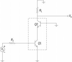
This is just two-domino gates operating on true and complement inputs with a minimized logic tree. Show more 5 Abstract—- In this paper, high performance carbon nanotube based Cascode operational transconductance amplifiers COTA have been designed and simulated. To get the fancied result, we should apply a standard based framework. The complementary metal oxide semiconductor CMOS technology is suitable for low power, high-speed analog and mixed signal circuit design. Cascode Voltage Switch Logic CVSL refers to a CMOS-type logic family which is designed for certain advantages. The first method for reducing the actuation voltage is to increase the electrostatic force.
Cascode voltage switch logic PowerPoint (PPT) Presentations, Cascode voltage switch logic PPTs
There are some problems arising from temperature- dependent to power supply rejection ratio when implementing a bandgap reference circuit. The perfomance of the proposed converter is analysed with the help of simulation results and the simulated effcency of the converter is found to be 94. The Cascode with the Output Open-Circuited. The proposed circuit modification principle, applied to a boost converter, is illustrated in the next section. If we modify DCVSL circuit by adding two weak p channel devices i. Based on the analysis of the measurement principles and methods of the TMR magnetic sensor, a current measurement system was designed which was applied in the high voltage switch board.
Static And Dynamic Cmos Cascode Voltage Switch Logic Circuits Computer Science Essay
The transient response voltage is set as 1 V with 0. VDD 0 to1 swing 0 a Switching waveform for single rail logic VDD 0 to1 swing 0 a Switching waveform for dual rail logic Fig 1 Switching action for single and dual rail network The slew rate is simply the rate of change of the output voltage in time. Among all these 2T Multiplexer is optimal. When a part of the circuit fails, the main function of the circuit can be realized by reconfiguring the pulse width modulation. For the recovery and recycle the supplied energy, an AC supply power is used for ECRL gates. The logic trees may be further minimized from the full differential form using logic minimization algorithms.
However, most of the reported RF MEMS comb switches have a DC contact and less capacitive contact. However, the demand for high-performance digital systems requires continuously faster CMOS circuit speed. The resulting converter, called BDHC, is the prime focus area of this paper. The solar energy is inverted and applied to the second winding of primary. The boost operation of the proposed converter can be realized by turning on both switches of any particular leg either S1—S4 or S3—S2 simultaneously. You can view or download Cascode voltage switch logic presentations for your school assignment or business presentation.
These are due to the deposition of dielectric on the side walls which limits the ON and OFF capacitance ratio. Diodes D1, D2, and D5 are turned off, and D3, D4, and D6 are turned on. The cross-coupled latch is provides complementary outputs and that is shown in Fig 4 A B C D E Q Fig 4 Simulation waveforms for static CVSL circuit Clock A B C D Q Fig 5 Simulation waveforms for dynamic CVSL circuit The dynamic CMOS cell designed CVSL circuit of the Boolean function is given byas a four XOR gate implementation. Get Help With Your Essay If you need assistance with writing your essay, our professional essay writing service is here to help! This dynamic cascade switch logic circuit allows with small aspect ratio for charge compensation without excessive current flowing onto the node. Show more 9 In this work, a highly effcient single- switch resonant boost converter with an energy-blocking diode was designed for use in a solar energy generation system. This endeavor proposes a new out of the crate new organization model maintained adaptable PI organization, which might self- switch the organization gets all through an unsettling impact.
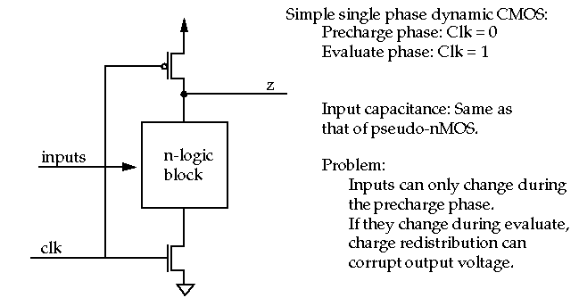
Therefore, the problems associated with brushes, for example, sparking, and wear and tear of the commutator assembly are eliminated. When a fault occurs, the faulted device is bypassed by switching on the additional SCRs in parallel with the power semiconductors. C Dynamic CVSL: The static CVSL logic gate can be transformed into dynamic circuit by rewiring the pFET latch to the clock-driven arrangement, shown in Fig 3. Simulation result and analysis The performance of the static and dynamic cascode voltage switch logic circuits designed and evaluated through cadence-gpdk90 nm technology. Both outputs are so generated that irrespective of the signal input, a constant load capacitance is derived by the power clock generator. Hybrid converter topologies can be synthesized by replacing the controlled switch with an inverter bridge network, either a single-phase or three-phase one.
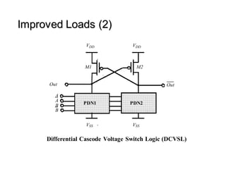
However if we control the inputs of pMOS transistors the peak voltage on the nets will be reduced to V DD -V tn during redundant operations. The threshold voltage of both pass-transistors should be identical for accurate operation. Politècnica de Catalunya, Barcelona, Spain Manchester University, UK University of Newcastle upon Tyne, UK. . If the converter is connected to a PV energy generation system with Constant Voltage MPPT control, the system can be used as a battery charger without any feedback controllers as the output voltage of the converter remains constant. A Dual rail Logic concept: The dual rail logic structure is consists of two-pFET are cross-coupled to form a simple latch that provides complementary outputs and; the latch is driven by an nFET network that can be viewed as two complementary switching functions. .
The conductions of the source-gate voltage on the devices are given as The behavior of the latches is that and is andare voltage complements in this circuit, so one is high while other is low. Also, as a consequence of the differential signals, which means an effective doubling of the voltage swing, CVSL is very robust against noise and against capacitive noise coupling. However, the output resistance has decreased in CNT based COTAs in comparison to conventional CMOS-COTAs. The logic design strategic is achieved in CVSL by cascading differential pairs of FET devices are capable of processing Boolean functions up to 2N-1 input variables within a single circuit delay. This special characteristic owns by FGMOS is definitely contributes towards low voltage and low power circuit design. Large Diffusion Connected Network DCN produces differential small signals. In practical the dual rail logic has some problems; increased circuit complexity, increased interconnects required in the layout and timing issues become critical.